By Ramish Zafar
Publication Date: 2026-10-16 07:52:00
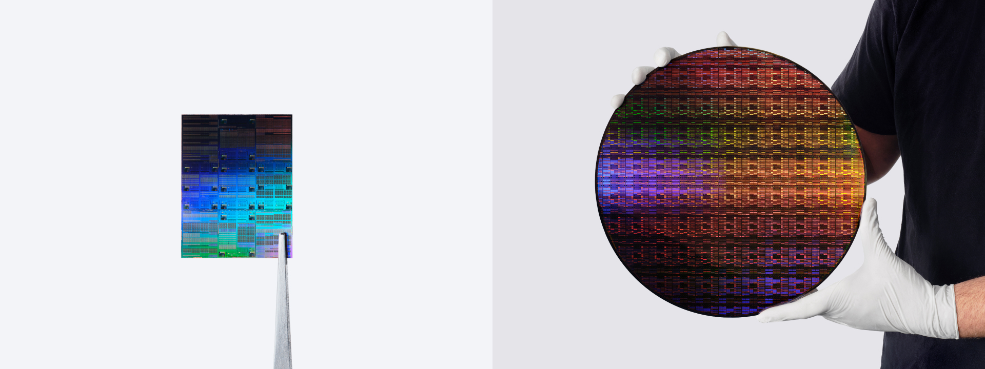
Computing giant International Business Machines Corporation (IBM) has made key progress with its next-generation chip manufacturing technology that seeks to bring significant improvements to compute and memory chips. The firm launched its 0.7-nanometer ‘Nanostack’ chip manufacturing technology in June, and now it has started to provide process development kits (PDKs) for the technology to those interested in the first quarter of 2027.
IBM Progresses With 0.7-Nanometer Technology To Enable Chip Firms To Familiarize Themselves With Tech Before Widespread Adoption
IBM’s 0.7-nanometer is an extension of current chip manufacturing technologies, of which the 2-nanometer is currently the latest one in mass production. After 2-nanometer, manufacturers such as Intel and TSMC plan to move forward to processes including 18A, A16 and A14. These three define the technology, in marketing terms, by relying on angstroms as notation with 1 nanometer equaling 10…


